We suppose, that you have read the theoretical notes for test generation and fault diagnosis in prior to read the following text. We also put a stress on the fact that all the everything here holds only in the situation when the design contains exactly a single design erorr in it. The design error model used in this work includes only gate substitution errors and missing/extra inverter errors. In other words either:
In our case, we are lucky to have yet another restriction. Using the prediagnostic tool, we obtain an intermediate diagnostic result, which enumerates (restricts) the list of suspected gates and stuck-at faults. We are talking about stuck-at faults because we are going to make almost all the work using this fault model. This model is widely used and there are a lot of various fault localization methods worked out for it. Therefore, it is a convinient model to work with. However, after the diagnosis is made on this model, it must be translated into the language of design errors. For this purpose, a combination of stuck-at faults at inputs of the localized gate corresponding to a certain gate replacement error is provided (see the table below).
What we initially know about our design is that its implementation is erroneous and that we have an abstract specification, which we consider as to be correct. We can apply test patterns to both the implementation and specification and measure the output responses of the both models. We also have the information about what part of the implementation contains the design error within. Gates, which are said to be suspected as erroneous are enumerated. Information about imaginary detected stuck-at faults (SAF) is also given.
Actually, we have some suspected gates and some combination of SAFs at the inputs of those gates. Our task is to diagnose the design by reducing both lists as much as possible, generating and applying special diagnostic test patterns. We are going to do this incrementally until it will be possible to derive hopefully a single suspected gate as the final diagnosis.
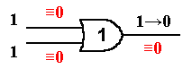
The elimination of SAFs is done using common single stuck-at fault diagnosis methods based on fault tables. However, a restriction holds, which is illustrated in the following figure.
Let's say there is the combination of SAFs shown in red color and we have a test pattern "11" at the input of the gate. The output response must be also "1", because of the logic function of OR gate. However, we observe "0" instead. So, the failure is detected! Note, that all the SAFs are activated by the given test pattern, but not all of them can be observed at the output. The two SAFs at the inputs are blocked by the OR gate and cannot be propagated towards the output. So, they cannot be observed. In such a case, the single-fault diagnosis theory tells us that the observed fault is the one at the output of the gate while the gate inputs are correct.
However, we must not believe it because the real error is not the SAF at the output of the gate but the gate itself. Moreover, the faults at the inputs are reperesentative faults for this gate replacement error (in our case, the correction is OR ->AND corresponding to the Table 1) and must not be eliminated! Instead of it, we must think of them as they were both present at the same time (multiple faults instead of a single one). This makes the OR gate transparent to both SAFs and changes the output value from 1 to 0 what is consistent with our observations. If there were the stuck-at 0 at the output it would be also consistent with the observations (it is an equivalent fault to those at the inputs). However, we cannot provide a conformity rule of such a SAF and an error from the design error model. So, we do not consider it.
It is always helpful to think of SAFs as "bundled" with the corresponding gate because these SAFs are only imaginary. The real cause of error is the logic gate. Keeping this in mind, we can safely use all the ideas described in the single-SAF-diagnosis theory. The following statement can be very useful in our struggle to locate the single erroneous gate. A stuck-at fault f, which is testable by a test pattern T can be eliminated from the set of suspected faults F if at least one of the following is true:
The first is quite intuitive. If we observe an error at some output, then the cause of the given observation must lie at the cone of influence of this output. Moreover, as the error is single, then no other errors exist in the design. If there are several erroneous outputs, then the error is located in the intersection of all the cones of influence of these outputs.
The second statement can be illustrated by the following example.
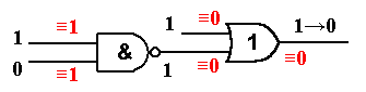
From this picture we see that the stuck-at 1 is activated at the second input of the NAND gate. This fault propagates up to the output of the NAND gate but not towards the primary output of the circuit (because OR gate is not transparent). This means that, if we observe an error at the primary output, the cause of this error is not the stuck-at 1 at the input of the NAND gate. This SAF must be eliminated from the list of suspected faults. The same holds for the stuck-at 1 at another input of the NAND gate (however it was neither activated, nor propagated).
If we consider this case from the point of view of the gate substitution fault model, then we can clearly see that by placing both "1" at the inputs of the OR gate we make it non-trasparent, which means all the faults located before the OR will not show at the output. I.e. the NAND gate is blocked! The error in this gate cannot be observed at the output, provided the OR gate is correct. But the error is observed. This means that, the OR is not correct. Moreover, only a single gate in the design can be erroneous (as was stated in the beginning). Therefore the erroneous gate is the OR.
All that was said above touches the case of erroneous output (fault is observed). Consider now the same test vector for the same circuit but the output was correct. What does it mean? In terms of stuck-at faults, all the activated and propagated (testable by the given test) faults are "correct". Speaking strictly, these fault are not present in the design. However, this test did not test much. Only the stuck-at 0 at the output is tested. We can eliminate this fault from our fault list. Unfortunately, it is not sufficient to test only the output for SAFs to be sure that the gate is correct.
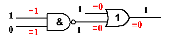
In the case of correct output all the single-fault diagnosis rules apply. This means that, we can hold that a corresponding signal line is fault-free if at least one of the following is true:
By applying this rules, we can eliminate whole gates from the suspected list because of the following statement:
– A gate is correct if at least one of the inputs of the gate is free from stuck-at faults².
Using this principle, it is sufficient to proove that one of the inputs of a gate is fault-free in order to proove that the whole gate is fault-free. In this way we can eliminate the gates one by one from the set of suspected erroneous gates. In other words, if we succeed to prove that at least one of the gate's inputs is fault-free, then the considered gate is correct and cannot be suspected anymore.
When all the gates are examined and a single erroneous gate is identified, we can use Table 1 (in the end of the document) to decide what kind of a gate replacement is needed to transform the implementation so that it will be functionally equal to the specification.
To sum up what was said above, let us discuss the following example. Say, we need to diagnose the circuit below and we know the combination of suspected stuck-at faults shown in red ("D" stands for both SAFs suspected at the same signal line). The suspected erroneous gates are G1, G2, G3, G4, G5, and G6.
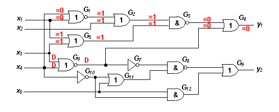
Our task is to use the ideas above in order to create such diagnostic tests, which allow to eliminate the gates one by one from the set of suspected erroneous gates. We will try to split the erroneous area everytime in two pieces and decide which part is correct and which is not. So, we will apply the sequential diagnisis approach.
The first thing we can notice in our case is that the different gates affect different outputs. Gates G1, G2, G3, G4, and G5 affect only the output y1 while gate G6 affects both. This means that, if the error was detected at y2, then the erroneous gate would be located. It would be G6 because no other gate affects y2. In order to check this, we must compose a test pattern that tests SAFs at G6 and propagates them to y2.
Three test patterns XX000, XX011, XX100 test all the four SAFs at the inputs of G6. If all of them fail (the fault is always detected at y2) then NOR gate G6 is erroneous with both SA 0 and SA 1 at the inputs, which corresponds to the correction NOR->OR. If the first pattern, which tests SA 1 at both inputs, failed and the other two patterns were okay, then the correction would be NOR->AND (since SA 0 is not any more suspected at both inputs). In the opposite case (first pattern was correct while the other two failed), the correction would be NOR->NAND. Let we have the case, where all the patterns gave correct results. Then gate G6 must not be considered as erroneous anymore. Remaining gates should be examined instead.
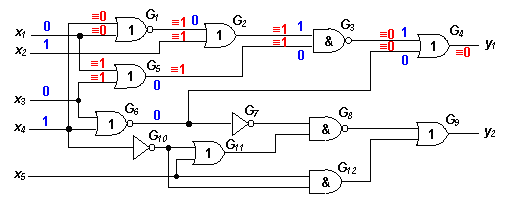
We are going to split the remaining area into two parts. The "0" at the second input of G3 blocks gates G1 and G2 so that all the possible errors in those gates will not show up at the output. At the same time we are going to test all the remaining gates for stuck-at faults. For this purpose we put corresponding values at the signal lines. The values, which test both inputs of G5, the second input of G3, and the first input of G4 are shown in blue. If the output was then faulty, the location of the error is somewhere in G3, G4, G5 because we tested them and the error was detected. Let's say that in our case the output was rather correct. Then the gates G3, G4, G5 are also correct because a gate is correct as soon as one of its inputs is proven to be correct. So we have to distinguish only between the two remaining gates G1 and G2. Let's concentrate on them.
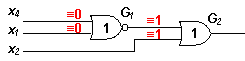
We have to options: either to test G1 while not testing G2, or to test G2 while not testing G1. However, it is not difficult to show that it is impossible to test one of the gates separately. On one hand, G1 is tested by vectors 01 or 10 or even 11 (the latter is true because there are both imaginary SA 0 at the same time). This gives 0 at the first input of G2. In order to make G2 transparent the second input of G2 must be 0 as well. These two zeros make gate G2 testable. Therefore, if we test G1, then we test also G2. On the other hand, if we want to test G2, we have to provide two zeros at the inputs of G2. That is, the inputs x4 and x1 must be either 01 or 10 or 11 what tests also gate G1. Therefore, if we test G2, then we test also G1. This means that, the maximum diagnostic resolution is achieved and we cannot distinguish between these two gates! However, we are eager to find the answer what gate is really erroneous and the following idea will help us.
What we need here is to
forget about stuck-at faults. They won't help us anymore. Consider the gates
as they are and try to guess which replacement is possible in our design. We
need to have a look at the Table 1, which suggests the replacement NOR->NAND
for G1 and the replacement OR->NAND
for G2.
|
|
|
|
|||
|
|
|
|
|
||
|
|
|
|
|
|
|
|
|
|
|
|
|
|
|
|
|
|
|
|
|
|
|
|
|
|
|
|
|
|
|
|
|
|
|
|
|
|
|
|
|
|
|
|
|
|
|
|
|
|
|
|
|
|
|
|
|
|
|
|
|
|
|
|
|
|
|
|
|
|
|
|
|
|
|
|
|
|
|
|
|
|
|
|
|
|
|
|
|
|
|
|
|
|
|
|
|
|
|
|
|
|
|
|
|
|
|
|
|
|
|
|
|
|
|
|
|
|
|
|
|
|
|
|
|
|
|
|
|
|
|
|
|
|
|
|
|
|
|
|
|
|
|
|
|
|
|
|
|
|
|
|
|
|
|
|
|
|
|
|
|
|
|
|
|
|
|
|
The following table presents the functions of NOR, NAND, and OR gates. From this table we see that the replacement NOR->NAND can be detected by the vectors 01 or 10.
|
|
|
|
NAND
|
|
|
|
|
|
1
|
|
|
|
|
|
1
|
|
|
|
|
|
1
|
|
|
|
|
|
0
|
|
The vectors 00 or 11 can detect the replacement OR->NAND. Therefore by placing the vector 00 to the inputs of G1 and the vector 11 to the inputs of G2 we test G2, but not G1.
Let's say the final test passed without any error shown up at the output. Therefore G2 is correct and G1 is erroneous. To rectify the design we must replace existing NOR gate by the NAND.
¹ An erroneous output is such an output where we observe the difference between the specification and the implementation in the way they are responding to an input pattern. The verify tool clearly shows the erroneous outputs marking them by the word "Error".
²
For details please read the following article:
R.Ubar, D.Borrione, "Localization
of Single Gate Design Errors in Combinational Circuits by Diagnostic Information
about Stuck-at Faults," Proc. of the 2nd Int. Workshop on Design
and Diagnostics of Electronic Circuits and Systems, Szczyrk, Poland,
Sept. 2-4, 1998, pp. 73-79
| |
Last update: 28 July, 2004